Abstract ---
Optical samples ---
E-beam samples ---
Description ---
Details (in Czech)
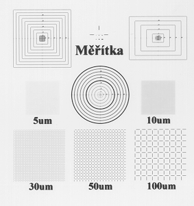
Dimension Standards for Electron and Optical Microscopy
prepared by Electron-Beam Lithography
Grid (3-100um) and geometric shape (rectangles, circles, scales) standards were prepared using electron-beam lithography. A high precision of the standards is due to a laser-interferometer based calibration of the exposition field. Samples were prepared for the optical microscopy (thin-film metal on glass substrate) as well as for the electrone-beam microscopy (e.g. anisotropic etching of Silicon). Required geometry and size can by designed according to specific user requirements.
Detailed information:
a poster at Transfer'99 conference
(in Czech) or upon request
(Matejka,
Kolarik)
|
|
